Earth is bathed in huge amounts of energy from the Sun—885 million terawatt hours every year. This is a lot—around 6,200 times the amount of commercial primary energyGLOSSARYprimary energyEnergy in natural sources that has not been converted into other forms by humans. used in the world in 2008. Humans have always used some of the Sun''s energy directly—for drying clothes and foodstuffs, for example. They''ve also utilised it indirectly—through photosynthesis to power the plant growth underpinning the agriculture that supplies us with food and the oxygen we breathe.
And there is another way to use this abundant energy source: photovoltaic (photo = light, voltaic = electricity formed through chemical reaction) solar cells, which allow us to convert sunlight directly into electricity. Since the demonstration of the first silicon photovoltaic cell in 1954, by Daryl Chapin, Calvin Fuller and Gerald Pearson at Bell Laboratories, New Jersey, we have been refining the technology that enables us to harness the reliable, free and clean energy from the Sun.
That first solar cell had an efficiency of around 5 per cent. Many years of solid work have seen that rise to generally around 20 per cent. Solar panels are appearing on more and more rooftops around our suburbs as solar photovoltaics (PV) become an increasingly viable option for domestic electricity production.
It has been known for more than 150 years that light can have an effect on the electrical properties of some materials. This is called the photoelectric effect. In 1921, Einstein received the Nobel Prize for his work explaining this. Photovoltaic cells are based on a related phenomenon called the photovoltaic effect, and they convert light directly into electricity. Let''s look at how.
Most photovoltaic cells are made of silicon, an element that is at the heart of all modern electronics. Silicon is special because of the arrangement of its electrons—it has four out of the possible eight electrons in its outermost shell. This means that it makes perfect covalent bonds with four other silicon atoms, forming a lattice structure.
This bonding mechanism means there are very few free electrons floating about, which is what we need to create electricity. That''s what electricity actually is, after all—the flow of electrons. Because of the arrangement of bonds in its crystal structure, silicon in its pure form doesn''t have very many free electrons, so we ''dope'' it.
Doping adds an impurity to the silicon to change the way its atoms are bonded together and share their electrons. Adding small amounts of phosphorus, which has five electrons in its outer shell, as compared with silicon''s four, means that the extra (fifth) electron has nothing to bond to, so it''s free to roam around and create electric current. Electrons have a negative charge, so when the silicon is doped in this way, it''s called a negative material: n-type.
We can also dope with boron, which has only three electrons in its outer shell. This leaves one of the bonds with only one electron, creating a ''hole'' in the bonding structure. Electrons within the boron-doped silicon can jump around to fill in the hole. Alternatively, the holes themselves can be thought of as moving (in the opposite direction to the electrons) as the electrons hop from one bond to another. This movement also constitutes an electrical current. We now have a material with an overall deficiency of electrons, making a positive (p-type) material.
The extra electrons and holes can float around the lattice; they are ''shared'' by all the atoms in the structure. This gives each doped material an overall slight preference to either give or receive electrons. This is known as electronegativity—a measure of how strongly an atom or material hangs on to its electrons.
However, when we put the p-type and the n-type materials in contact with each other, something interesting (and useful) happens. At the point where the two types meet—the junction—electrons from the n-type layer diffuse over into the p-type layer, leaving behind an area with a slight positive charge in the n-type layer. The reverse happens in the p-type layer—holes diffuse into the n-type layer, leaving behind a slight negative charge in a region of the p-type layer. This creates an electric field, which will direct the flow of electric current.
Now, consider a photovoltaic cell made from a wafer-thin combination of p-type silicon laid over a layer of n-type silicon. When sunlight hits our cell, the energy of its photons excites electrons into states called ''electron-hole pairs''. When these are formed in the vicinity of the electric field at the junction of the p- and n-type layers, the electric field pulls the pair apart (they form a ''charge-separated'' state). Controlled by the force of the electric field, the electrons travel to the n-type side, and the holes to the p-type side.
The photons'' energy can also create electron-hole pairs in other parts of the doped silicon. Sometimes, these electron-hole pairs will simply pair up again (recombine) with the extra energy emitted as heat. But if they find themselves near the electric field at the junction of the p- and n-type layers, the electric field will send electrons to the n-type layer, and holes to the p-type layer.
If you create an external connection (using electrodes and a wire) between the two layers, the electron will then travel back through the wire to the p-type layer, as an electric current that does useful work. The whole thing acts rather like an electric battery, continually recharged by the sunlight.
Silicon is the most common go-to material for a photovoltaic cell because the maximum wavelength of energy it absorbs is around 800 nanometres, which is close to the peak of the radiation emitted by the Sun. The Sun emits a spectrum of radiation, ranging from around 300 nanometres to 2,000 nanometres, but by far the majority of it is within the range of 420 to 700 nanometres.
The reason why phosphorus and boron are most often used as the doping agents is a bit more complicated. In order to create the flow of electrons within the solar cell, the electrons must be excited out of their stable ''ground'' state up into the higher energy level needed for them to move from the p-type to the n-type side. This amount of energy is equivalent to the difference in electronegativity between the two layers (this is called the band gap). Any less and it won''t be enough to ''knock'' the electron free, and any extra energy would be wasted.
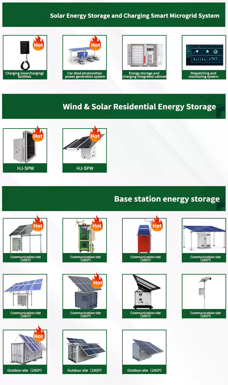
About Solar energy to electrical energy
As the photovoltaic (PV) industry continues to evolve, advancements in Solar energy to electrical energy have become critical to optimizing the utilization of renewable energy sources. From innovative battery technologies to intelligent energy management systems, these solutions are transforming the way we store and distribute solar-generated electricity.
When you're looking for the latest and most efficient Solar energy to electrical energy for your PV project, our website offers a comprehensive selection of cutting-edge products designed to meet your specific requirements. Whether you're a renewable energy developer, utility company, or commercial enterprise looking to reduce your carbon footprint, we have the solutions to help you harness the full potential of solar energy.
By interacting with our online customer service, you'll gain a deep understanding of the various Solar energy to electrical energy featured in our extensive catalog, such as high-efficiency storage batteries and intelligent energy management systems, and how they work together to provide a stable and reliable power supply for your PV projects.
Related Contents

